Saturday, November 12, 2011

WT40, Part 5: BUILDING the AUDIO AMPLIFIER MODULE


WT40 Part 5:  BUILDING  the  AUDIO  AMPLIFIER  MODULE


There have been some minor updates to the Schematics and Layout Drawings shown in previous posts to this blog.

Revised drawings are shown below.


For the benefit of inexperienced builders, much detail will be presented for building the Audio Amplifier Module because this is the first module in to be built in this series.   It is not my intention to insult anyone's intelligence by dwelling on boring details, and I think it is equally important to present enough information so that nobody gets lost in the process.

Subsequent modules will omit some of the detail.

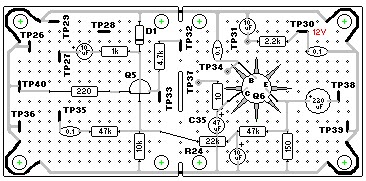
For the subject at hand, which is building the Audio Amplifier module, an updated Schematic for the Audio Amplifier Module, which includes both Preamplifier  and  Amplifier circuits, is shown below.


Incoming signals will be carried by a twisted pair (or by miniature coaxial cable, such as RG174 or equivalent, if you prefer).  Notice on the Schematic Drawing that signal points, such as the one for Audio In, require TWO Tie Points: one for the signal (TP27) and a companion Ground connection labeled (TP26, or other Ground Tie Point of your choice).
                             
The Layout Drawing shown below is one of many that work equally well.

Notice the Orientation of the 276-148 Circuit Board - - the "short" end (213 perforations) is to the left and the "long" end (228 perforations) us to the right.


The layout drawing shows TOP views of components in black.  The gray lines show the connections on the Solder Side of the circuit board - (sort of) an "X-Ray" view.

Notice, in the upper lefthand corner of the Layout Drawing, the Tie Points for the Incoming Audio Signal, TP27, and it's companion Tie Point for Ground, TP26.

In the Schematic Drawing, notice that TP27 connects to the Wiper of the Audio Gain potentiometer, R17, which will be mounted on the control panel for the transceiver.  The Grounded end of R17 connects to TP26, which connects directly to the Ground Buss.  The other end of R17 connects to TP28, which will also have a second wire carrying the Audio Signal connected from either the Product Detector or the (optional) audio Filter.

This means that TP28 is the audio signal from the Product Detector module enters the Audio Amplifier module - - even though there is no connection shown on the Layout Drawing.

Now, let's take a  look at a . . .

PROCEDURE  FOR  BUILDING  the  AUDIO  AMPLIFIER  MODULE
[Applies to all modules.)


The procedure shown here assumes that the Radio Shack #276-148 Dual Printed Circuit Board, or equivalent, is being used as the platform on which the modules will be built.

A  5-STEP  BUILDING PROCEDURE:


[1] Collect all parts required for the module.

[2] Prepare the circuit board.

[3] Populate the circuit board.

[4] Perform initial check-out of the circuit board:
     [] Visual Check
     [] Resistance Measurements
     [] Current Measurements
     [] Voltage Measurements

[5] Operational Test

Here in Part 5, we will complete items [1], [2],  and [3] in the procedure, then perform Visual Check-Out and Resistance Measurements.

Current and Voltage Measurements and a preliminary Operational Test will be done in Part 6.  The final operational test will be done after all the receiver modules have been completed and assembled.

NOTE:  Jumper Wires will be soldered in place during  Measurements in Part 6.

A final Operational Test wil be done after all the receiver modules have been completed and assembled.

I recommend you have all parts on hand, as suggested in Part 4, before starting to . . .


PREPARE  THE  CIRCUIT  BOARD


FIRST,   Mount Standoffs at each corner of the Radio Shack #276-148 Dual Circuit Board, or equivalent.


At this point in the process the standoffs will be serving as anchors at each corner for mounting the Ground Buss, which you can see looping around the standoffs in the photo, above.  The recommended standoffs are:

[]  1/4 inch long Hex 6-32 Threaded Male / Female standoffs, JAMECO #133542, or equivalent, on the Solder Side of the circuit board.

[]  5/8 inch long Hex 6-32 Threaded Female / Female standoffs, JAMECO #77552, or equivalent, on the Component Side of the circuit board.

Much later in the building process, when the circuit boards are mounted in their final configuration, the standoffs can be easily removed and replaced with different length standoffs, if required to accommodate the needs of the configuration.

ADDING THE  GROUND  BUSS

When the standoffs are in place,  ADD  THE  GROUND  BUSS, using about 11 1/2 inches of #22 bare copper wire.


As you can see in the photo, the Ground buss loops around the entire circuit board.

At each corner, the Ground Buss passes through a perforation, goes around the standoff, then passes through another perforation back to the solder side of the board, then continues around the entire board, looping around the standoff at each corner.

Where the two ends of the Ground Buss meet, there should be about 3/8 inch overlap where the two ends are soldered together.


TIE  POINTS

Each circuit board will have several TIE  POINTS.  These are labeled TPx in the layout drawing, shone below.  The number "x" is for identification.

                                                                                     
NOTICE that the circuit board is oriented with the "short" side containing 213 perforations to the left.

Tie points serve three functions:

[] Connecting points between modules
[] Test points for module check-out
[] Terminus for jumpers within a circuit board.  TPs for jumpers are, sometimes, simply a perforation in the circuit board through which a wire is passed and soldered to a component.

Tie points are shown on Layout Drawing in two forms:

[1]  Bold black lines between two adjacent perforations . . .


[2]  Gray circles around a single perforation . . .

The gray circles simply show where to insert one end of a Jumper Wire through a perforation.


The bold black lines between two adjacent perforations in the Layout Drawing represent a loop of #22 bare copper wire that has been fashioned into a Tie Point, as illustrated below.


A wire loop type Tie Point requires about 2 inches of #22 bare copper wire folding it into a "u" shape so it can be inserted into two adjacent perforations.

NOTE:  It is important that the bare copper wire is free of corrosion so that the solder adheres tightly to the wire.  If there is any discoloration to the wire, clean it with very fine sandpaper,  steel wool, or other fine-grained abrasive material.

Twist the wire on both the component side and the solder side, as illustrated in the drawing, above.

Form the wire to make a "U".  I find it best to form the "U" before cutting the Tie Point from the end of the wire.


Cut the wire to get a long, skinny, upside-down "U".


Insert the "U" into two adjacent perforations, then twist the wire on both sides of the circuit board.

The photo, below, shows a newly formed "U" that has been inserted into the circuit board to become a Tie Point for connecting to Ground, such as TP39 on the Audio Amplifier module.


Tie Points that are Ground Connections, such as TP39, are placed in the perforations nearest to an edge of the circuit board, as shown above.

A couple of twists on both sides of the circuit board will secure the Tie Point.


The photo below shows a Ground Tie Point soldered to the ground buss.


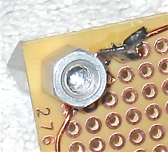
Allow about 30 seconds, or so, for at the solder to cool, then solder the Tie Point on the component side of the circuit board.  Notice, in the photo below, that the loop portion of the Tie Point is tinned with solder.


Tie Points that are NOT connected to ground, such as TP38, are placed so there is one or more perforations between them and the ground buss.


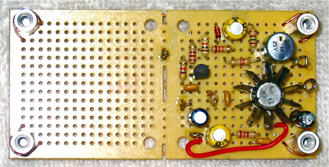
POPULATING THE CIRCUIT BOARD

The order in which the components are placed on the circuit board is a matter of personal preference.  I started by placing the 2N3053 and its attached Heat Sink onto the circuit board, then added the components and tie points (installing JUMPERS will be discussed, later).


PREPARING THE 2N3053 TRANSISTOR

The 2N3053  is an NPN Bipolar transistor housed in a TO39 metal case with three "legs" that allow connection to the Emitter, Base, and Collector; left to right in the photo, below.


The "legs" on the 2N3053 are formed before being inserted into perforations on the circuit board, as shown below, with the Emitter, Base, and Collector identified.

Notice, in the photo below, that the Collector leg is connected directly to the  case that houses the transistor.


This is IMPORTANT because it means that voltage is present on the case when voltage is applied to the circuit, and the case and the heat sink must not touch any other component on the board.

Form the legs so that the 2N3053 will stand about 3/16 inch above the circuit board.

When the legs are formed properly, attach the Heat Sink before inserting the transistor into the circuit board so that the legs will stand about 3/16 inch above the circuit board, as shown in the photo, below.


The Layout Drawing below shows the position of the perforation where the Emitter leg of Q6 is inserted through the circuit board.


The leg from the Emitter is inserted into the perforation located 8 perforations from the right end of the board and 7 perforations up from the bottom.

Shown below is a top view of the 2N3053 mounted on the circuit board - - with the Heat Sink Removed - -  to indicate where the legs pass through to the Solder Side of the circuit board.  The Base leg is soldered to the jumper wire coming from the Collector of Q5.  This solder joint is designated TP34 on the Schematic and Layout Drawings.


This photo was taken after one end of Jumper 6 (the blue wire) had been soldered in place at TP34.


Components can be added to the circuit board in any order you wish.  I recommend installing and soldering C36 from the Emitter of Q6 to TP38 next in order to hold Q6 firmly in place.

Be sure to orient C36 with the POSITIVE side connected to the  Emitter of Q6.

NOTE:  Not all electrolytic capacitors are polarized,  but  the ones use in the Audio Amplifier module ARE  POLARIZED.  It seems a bit strange that the positive connection of a polarized capacitor is indicated on schematic drawings while the negative connection is indicated on the body of the capacitor.   - -  Just one of the strange little quirks of "standardized" notation used in electronics.

On the Solder Side of the circuit board, the leads from components are formed firmly against the board with about 3/16 inch overlap, excess wire trimmed, then soldered.

The other connection to Q6 that will help hold it in place is C35, the 47 uF electrolytic capacitor that goes from the Collector to the Ground Buss, with the positive side of the capacitor to the Collector.

NOTICE in the layout drawing that the wire from the Negative side of C35 will pass under the 22k resistor R24 on the Solder Side of the board on its way to the Ground Buss.

Proceed to populate the remainder of the circuit board however you wish.  Take your time and double check all connections before applying solder.  Correcting wiring errors is sometimes necessary, but it is not much fun.

When the components are all in place, it is time to solder ONE END of the jumpers to the circuit board:  Jumper 4 (about 3 1/2 inch of insulated hookup wire) to TP30;  Jumper 5 (about2 inches of insulated hookup wire) to TP31;  Jumper 6 (about 1 3/4 inch of insulated hookup wire) to TP34.

Strip about 1/4 inch of insulation from each end of the jumper wires, and apply a light coat of solder to the bare wire.  If you are using stranded hookup wire, twist the exposed strands tightly together before applying the solder for "tinning".

Be sure the unconnected end ends of the jumpers do not touch the circuit board or any component on the circuit board.


Why connect only one end? (You might want to know.)  Because we have not yet done Current & and  Voltage Measurements, which will be done in Part 6.

The "other" end of the jumpers will be soldered in place as Measurements are completed in Part 6.

The color of the insulation is, of course, arbitrary.  I use red wire to carry 12 volt power; black, green, or gray for Ground; and some other color for signal connections.


INITIAL  CHECK-OUT

A Few Words Regarding Testing - - -

Each module will be tested to make sure it is functioning properly before being connected to other modules for operational testing.

A generic test procedure:

[] Visual Check to make sure all the components are present and properly soldered into place.

[] Resistance Check will reveal "short" (Zero Ohms) circuits and "open" (No Continuity) circuits.

[] Current Check to be sure excessive current is not being drawn, or that no current is being drawn in a circuit that should be drawing current.

[]  DC Voltage Check to be sure the proper voltages are present at key points in the circuit.

[] AC current and voltage checking for signal processing modules.

[] Operational check to be sure the module if functioning properly.


The most likely cause of problems on a newly built circuit is a WIRING ERROR of one kind or another.

Wiring Errors include:
[] Missing  components
[] Components not connected
[] Components connected to the wrong place
[] Connections not soldered
[] “Cold” solder connections
     - insulation material, such as enamel, not removed before soldering
     - not enough heat applied to flow the solder
     - mechanical shock or movement before the solder solidifies
[] Solder “bridges” causing a “short” circuit between two solder joints.

Initial Check-out Includes:


[] Visual Inspection
[] Resistance Measurements

VISUAL  INSPECTION

Begin your check-out with a thorough VISUAL INSPECTION to make sure that there are no missing parts, and that components are connected correctly, and properly soldered.  Defects will, of course, become obvious during resistance, current and/or voltage checks, but a good visual check can often spot errors that can be quickly and easily corrected before electronic testing begins and, thus, save a lot of time.

Begin your Visual Inspection with a COMPONENT  COUNT.

[]  On the Component Side of the circuit board, you should find:

    []  Three Jumper Wires CONNECTED AT ONLY ONE END.  (The unconnected end of the         jumpers will be used as test points during Resistance Measurements, below, and during Current &  Measurements in Part 6.)
    []  Two Transistors, a 2N3904 and a 2N3053.  The 2N3053 should have a heat sink attached.
    []  Ten 1/4  Watt resistors.
    []  Three 0.1 ceramic capacitors.
    []  One 1N4148 diode.
    []  Three 10 uF electrolytic capacitors.
    []  One 47 uF electrolytic capacitor.
    []  One 220 uF electrolytic capacitor.
 
If you find a discrepancy in component count, use the layout diagram and/or the schematic to find the error.

[]  On the Solder Side of the circuit board, check to see that all components are correctly connected and properly soldered.  I use a magnifying glass for this check because I have found that magnification sometimes shows problems that I would miss with the naked eye.  Finding a wiring error or a bad solder joint with a visual check is a heck of a lot easier than tracking it down during resistance, current, or voltage checks.

Correct any errors found during the visual inspection, then proceed to resistance measurements, below.

RESISTANCE  MEASUREMENTS . . .
 . . .  to verify that components are correctly connected and properly soldered in place.

Before doing resistance measurements, set your DMM to its lowest resistance scale, connect the two test leads on your DMM together, them observe and record the value shown on your meter.  This is the  "Zero" Ohms value for your meter.  On meters I have used, it is usually somewhere between 0.0 to 0.5 Ohm.

Some meters have provisions for adjusting so the meter will read zero for a dead short.  If your meter has such an adjustment, simply set it to Zero with the test leads connected together, and you are good to go.

Unless specified otherwise, resistance measurements are taken from the POINT INDICATED to the GROUND BUSS.

Resistance values are specified in Ohms;  k  =  X 1,000

Resistance Measurements  (other than ZERO and OPEN, which should be CRRECT or NOT CORRECT)  are OK if they are within plus or minus 10%.  If your measurements are off more than 20%, you probably have one or more wiring error.


[] TP40 to Ground Buss . . . .  Zero
NOTE: Now that you have verified that TP40 is connected to the Ground Buss, TP40 can be used as your GROUND POINT for Resistance Measurements.


[] TP26  . . . . . . . . . . .  Zero
[] TP27  . . . . . . . . . . .  Open, No Continuity
[] TP28  . . . . . . . . . . .  Open, No Continuity

[] TP29  . . . . . . . . . . .  Zero
[] TP30  . . . . . . . . . . .  No Measurement at this time
[] TP31  . . . . . . . . . . .  Open, No Continuity
[] TP32  . . . . . . . . . . .  Open, No Continuity
[] TP33  . . . . . . . . . . .  Open, No Continuity
[] TP34  . . . . . . . . . . .  Open, No Continuity
[] TP35  . . . . . . . . . . .  Open, No Continuity
[] TP36  . . . . . . . . . . .  Zero
[] TP37 . . . . . . . . . . .   Open, No Continuity
[] TP39  . . . . . . . . . . .  Zero


NOTE:  You have probably noticed on the Layout Drawing that TP28, which is the Entry Point into the Audio Amplifier module, does not connect to anything on the circuit board.  This may seem rather strange at first glance, but a quick inspection of the Schematic Diagram shows what is going on.  Before the signal enters the circuit board it passes through R17, the Audio Gain potentiometer, which will be mounted on the Control Panel of the Transceiver.  (More about mounting potentiometers when we get to Building the Control Panel.)

TP28 provides a place to connect the signal wire from the Product Detector to the signal wire going to R17.

R17 will not be connected into the circuit until we get to Operational Testing, but it does no harm to plan ahead.

Continuing with Resistance Measurements . . .

NOTE: The three measurements, immediately below, are between two test points, NOT to Ground.

[] TP30 to TP32 . . . . . .  2.2k
[] TP30 to Q6 Collector  . . . . . .  Open, No Continuity
[] TP30 to Q6 Base . . . . . .  Open, No Continuity


 Measurements on transistors, below, are from the leg indicated to Ground.

  Q5, 2N3904
[] Emitter  . . . . . . . . . . .  220
[] Base     . . . . . . . . . . .   8.6k
[] Collector   . . . . . . . .   Open, No Continuity

    Q6, 2N3053
[] Emitter  . . . . . . . . . . . 148
[] Base     . . . . . . . . . . .  Open, No Continuity
[] Collector  . . . . . . . . .  Open, No Continuity

Correct any errors found during Resistance Measurements before proceeding to Current & Voltage Measurements, and initial Operational Test in Part 6.

NOTE for those brave souls (especially inexperienced builders) who are attempting to build this module: If you have questions, comments, or suggestions, please email - - -
  or simply leave a comment in the space provided on this Blog.


             -  END of Part 5 -

Thursday, September 29, 2011

Part 4: AUDIO AMPLIFIER Continued . . .


I have no idea why I could not get this into the previous blog entry - - the graphics part of the Blogspot system just seemed to freeze up and would not let me enter any more photos.

One of life's little mysteries, I suppose.

F Y I:  The photo, below, shows an electronically identical, more compact version of the Audio Amplifier module that experienced builders can fit onto half of a 276-148 Dual Circuit Board.

   An even more compact module can be built by rearranging the layout and mounting components on both sides of the circuit board, but that's a story for another day.

One of the many benefits derived from building your own electronic circuits is that you can , within certain limits, build them to satisfy your particular needs.

Worthy of note in both the above photos is the Ground Buss wire, which you can see looping around the standoffs at each coiner of the boards.  The ground buss runs around the entire circuit board on the solder side of the board - -  you can also see tiny bits of it where the wire crosses the perforations in the middle of board.

The version of the WT40 Audio Amplifier using BOTH HALVES of the dual circuit board for the Audio Amplifier is the one that will be detailed in Part 5: Building the Audio Amplifier.


When things quit working as I was trying to enter the previous posting of Part 4, I was about to post the Flow Chart of the Receiver Section, showing where the Audio Amplifier fits into the the Receiver section of the WT40 Transceiver, so here it is . . .


Not surprisingly, the Audio Amplifier is the last module in the string before the signal goes into the earphones, then into your ear.

Notice that there is an Optional Audio Filter included in the drawing, along with an optional connection for a speaker.  Details for the filter and speaker connection will be presented when we get to Optional Features.

Meanwhile . . .

The FIRST STEP in building a module is to GATHER all the PARTS.

RULE OF THUMB: Never, ever, start building a module until all the parts are on hand.


PARTS LIST for the Audio Amplifier Module

The Parts List shown below contains only the parts required for the Audio Amplifier Module.


Resistors
1/4 Watt, plus or minus 5% tolerance.
Values shown in Ohms;  k = x 1000.

[] One:  10
[] One;  150
[] One:  220
[] One:  1k
[] One:  2.2k
[] One:  4.7k
[] One:  10k
[] One:  22k
[] Two:  47k

NOTE:  Quarter Watt resistors can be purchased for a penny each, or less, from parts suppliers such as JAMECO and MOUSER,  - BUT - to get such a good price, they must be purchased in lots of 100, or more pieces.  For small projects, such as the WT40 Transceiver, it is probably less expensive to pay the "extra" few cents to purchase them in smaller quantities.

Audio Gain Control
Plus or minus 20% tolerance,  1/4 Watt, Audio Taper Potentiometer (logarithmic).

[] One: 10k,  JAMECO # 255426, or equivalent.

NOTE:  The Audio Gain potentiometer mounts on the Control Panel, NOT on the circuit board, but you might as well add it to your parts collection now because you will need it during check-out of the Audio Module.

Another NOTE:  You may be wondering . . . What about a knob for the potentiometer?  That's a good question.  Actually, no knob is needed at this point in the game because the shaft is easily turned without a knob.  Knobs and switches will be detailed when we get to the Front Panel, much later in this series.  You can, of course, get a knob now - just be sure it will fit the shaft on the potentiometer you choose for Audio Gain control (the shafts come in different diameters, and some are slotted or half-moon shaped).

Capacitors:
Plus or minus 20% tolerance, Monolithic Ceramic, Type Z5U, or equivalent.

[] Three:  0.1 uF

Polarized, Electrolytic  Capacitors
Plus or minus 20% tolerance, Radial -Lead, rated for 16 volts or more.

[] Three:  10uF
[] One:  47 uF
[] One:  220 uF

NOTE:  Polarized electrolytic capacitors of a given capacitive and voltage rating come in different physical sizes.  I suggest you obtain the smallest size available from your parts supplier (Excluding surface - mount capacitors, which is story for another day).

Miscellaneous Parts

[] One: Radio Shack #276-148 Dual Circuit Board, or equivalent .

NOTE:  The "Front End" of the receiver (Filter, RF Amplifier, Mixer, and Audio Buffer) will require three or four more circuit boards.  I say "three or four" because I have not yet decided exactly how to package the circuits.  You will need a minimum of three, and a maximum of four for the receiver section of the transceiver.

Another NOTE: I have found that not all Radio Shack stores stock these circuit boards, so it would be good to call before going to the store.


[]  Mounting Hardware for the circuit board.  The exact hardware for mounting the modules will depend upon how the builder (YOU) decide to package your transceiver.  At this point in the building process, the main purpose for the standoffs is to provide an Anchor at each corner of the circuit board for the Ground Buss.  The standoffs listed here will be useful during final assembly of the transceiver, no matter what packaging procedure is used.
    [] Four: 1/4 inch, Hex 6-32 threaded, male/Female standoff, 1/4 inch long,  JAMECO #133542, or equivalent.
    [] Four: 3/4 inch, Hex 6-32 threaded, Female/Female standoff, 5/8 inch long  JAMECO #77623, or equivalent.

[] One: Heat Sink for the 2N3053 transistor, MOUSER part number 532-323005800, or equivalent.  Most any heat sink for a TO39 transistor will do the trick.  "TO39"   simply means "Transistor Outline number 39", referring to a  line drawing that shows the outline of the transistor.  The 2N3904 transistor used for the preamplifier is a TO92, and needs NO heat sink.

You can fashion a heat sink using #20 or #22 bare copper wire that is adequate for this application, as shown in the photo, below.


A wire heat sink requires the transistor to have a metal case so the heat sink can be soldered to the case.


Making a heat sink this way is a rather labor intensive task, and requires a bit of practice to get the wire shaped "just right", so it is not a job to be taken lightly.


Well, enough of that,  back to the parts list . . .


[] About 19 inches: #22 bare copper wire for the Ground Buss and Tie Points.  (And another six inches, or so, if you plan to make your own heat sink.)

NOTE:  You will use several feet of #22 bare copper wire for Ground Buss and Tie Points if you build all the modules in this transceiver following the procedure outlined here.  Bare copper wire can usually be purchased for less money at a hardware store than at an electronics parts store.

[] About 6 inches: #24 or #26 Stranded Hook-Up Wire for Jumpers.

Speaking of Jumpers, if you don't already have them, it would be a good idea to get set of test / jumper cable, Radio Shack # 278-1156, or equivalent.


[] About a foot, or so, of 3-wire hook up cable (sometimes called "intercom cable") to connect the Audio Gain potentiometer to the Audio Amplifier module during testing.  I use salvaged, multi-color ribbon cable for this sort of thing because wire of any kind is usually sold by the pound and/or in spools of 100 ft or more, which is a lot of wire, and it would take a couple of lifetimes to use up a 100 ft spool of of #24 or #26 hook-up wire (unless you plan to do an awful lot of wiring).  You may be able to buy wire by the foot at your local electronic parts outlet, and some Radio Shack stores still stock wire to sell by the foot - - ask for the 3-conductor intercom wire, #278-871.  

This intercom wire cable may (or may not) be available at your friendly, neighborhood Radio shack store.  There are several Radio Shack stores in the area where I live, and I have found that some stores carry a larger variety of items than others.

NOTE:  3-wire intercom cable, or equivalent, will also be need for testing of the Product Detector and VFO modules.  This cable comes in handy for all sorts of things at the workbench, so you might as well stock a few "extra" feet for future use.

THE  AUDIO  AMPLIFIER  CIRCUIT

A schematic diagram of the audio amplifier circuit is shown below, along with a drawing of a suggested layout.


This audio amplifier circuit has been published in several editions of the ARRL handbook, and is intended primarily for use with headphones.

A few things worthy of note in the Schematic Diagram and the Layout Drawing. . .


[]  The Schematic is intended to represent the Electronic Circuit, not he physical layout, which is the job of the Layout Drawing.  The schematic is more "absolute" than the layout drawing, which is more of a suggestion.

[]  The LABELING and NUMBERING of COMPONENTS is somewhat arbitrary, but not random.  TP27, TP28, TP29, etc. represent Tie Points,  which can also serve as Test Points.

[]  Some of the Tie Points, such as TP31,  are represented by GRAY circles, and are different from other tie points in that they are simply perforations in the circuit board where hook-up wire is inserted so it can be soldered to a component on the solder side of the board.  These tie points are used (mostly) the ends of Jumper Wires.

[]  The Tie Points represented by a dark black line between two perforations, such as TP40 (a Tie Point for Ground) and TP35 (a Tie Point for the Sidetone Signal) are fabricated using #22 bare copper wire.  A detailed description of how to make these tie points will be included in Part 5: Building the Audio Amplifier.

NOTE:  The symbols I am using for Tie Points are NOT industry standard symbols - they are a way to help me keep track of what's going on n the circuits, and I hope they are also helpful for you.

[]  Components other that Tie Points are also numbered sequentially, such as R22, R23, and R24, which represent RESISTORS.  There are two types of resistors represented in this Schematic:
       [] R17, which is a variable resistor (potentiometer) used as a Volume control, which has Three connecting points, TP26, TP27, and TP28.
       [] All other resistors, which are Fixed Value resistors, have Two connecting points, one on each end.

NOTE:  R17 is NOT mounted on the Audio Amplifier circuit board - it will be mounted on the Control Panel of the transceiver, and connected to the circuit board with hook-up wire.  I have included R17 in the Audio Amplifier schematic because it is an important part of the circuit, and helps show, exactly, where the signal entering the Audio Amplifier at TP27 comes from.

[]  There are Two types of CAPACITORS used in the Audio Amplifier module:
      [] C29, C31, C34, C35, and C36 are Polarized Electrolytic Capacitors - easily recognized because of the "+" designation on the positive end of the capacitor, and a (slightly) different symbol than . . .
      [] All other capacitors, which are much smaller, non-electrolytic Ceramic Capacitors.

[]  There are Two types of TRANSISTORS:
      []  Q5, a 2N3904, small signal transistor that serves as the PREAMPLIFIER to boost the signal to a suitable level to be amplifier by . . .
      []  Q6, a 2N3053, which can handle more power than the 2N3904, and power a set of Headphones.

NOTE:  Both the 2N3904 and the 2N3052  are bipolar, NPN type transistors.

[]  The Diode, D1, a 1N4148, helps stabilize the preamplifier.

If you what or need more details about Symbology, Terminology, and Definitions regarding Schematic Diagrams, the ARRL Handbook is an excellent reference.

Alert readers, such as yourself, will have noticed that the items enumerated in the Audio Amplifier, C29, C30, C31, etc. begin with two digit numbers as opposed to 1, 2, 3, etc.  This is because I have numbered the components in the entire Receiver Section, including the Receiver Filter, RF Amplifier, Mixer, Audio Buffer, and Audio Amplifier to follow the signal flow through the modules from antenna input through the Audio Amplifier.


I was planning to include a Schematic Diagram of the entire Receiver section of the Transceiver at the beginning of Part 5, but since Part 4 has been split into two entries into this blog, I might as well include it here, for your reference.

If you are not accustomed to working with schematics, this diagram may appear a bit overwhelming.  Keep in mind that we will be dealing with small parts of the circuit - one relatively small module at a time, such as the schematic for the Audio Amplifier which appears earlier in this post.

CAVEAT:  I'm still working on some minor changes in the modules preceding the Audio Amplifier, so the enumeration of items may be slightly different than shown here but the time I post Part 5 here on this blog.

Be that as it may, I will keep readers of this blog informed as to what is going on.

Component numbering for the VFO, the Transmitter section, and Optional Features will have their own component numbering scheme,  each beginning with 1, 2, 3, 3  etc.

Come ti think of it - - I may go to a fresh numbering for each module because it is time consuming and boring when I have to go through the whole schematic and layout drawing to re-number the components.   Hmmm m  m . . .  I'll have to think about that, some more.

No, I do not use a schematic generating application program to draw the schematics and layouts you see here - I do it all with the keyboard and mouse, one component at a time to create a bitmap file using Paintbrush, then convert the graphics to PNG  format for posting.  Google Blogspot probably converts the graphics to format before placing them onto the blog, and I have no control over that.

OK, that finishes Part 4.


Collect the parts for the Audio Amplifier module in preparation for Part 5: BUILDING the AUDIO AMPLIFIER where we will actually power up the soldering iron and do a bit of soldering.

Speaking of soldering . . . if you are new to this game of building electronic circuits, I recommend reading the Circuit Construction chapter in the ARRL Handbook.  Yes, the whole chapter, paying particular attention to the sections about assembling components onto circuit boards and soldering.

One way to gain some experience with soldering techniques is to fabricate several small copper wire rings, about half an inch, or so, in diameter.  I think such an exercise will prove to be worthwhile when you start preparing and populating the circuit board in Part 5.


       END of Part 4:   AUDIO AMPLIFIER MODULE, an INTRODUCTION


Wednesday, September 28, 2011

Part 4: AUDIO AMPLIFIER MODULE an INTRODUCTION


Building of the WT40 Transceiver will begin with the Audio Amplifier module and proceed "backward" through the modules until we get to the antenna connection.


For just about everything you do in electronics there are at least two ways to do it; sometimes there are dozens of ways to accomplish the same thing.  This means choices must be made.  For the purpose at hand, I have made some of those choices for you.  I have chosen to use discrete components for the Audio Amplifier because I think discrete components are easier to work with.

The audio module for the WT40 is a relatively simple, low-power circuit, shown in a photo of the prototype,  below.


The red jumper wires on the circuit board are for distributing 12 volts to power various parts of the board.

The blue wire is a jumper to carry the signal from the output of the preamplifier transistor to the base of the amplifier transistor.

The "legs" on the 2N3053 transistor are pre-formed before the heat sink is mounted, then the transistor placed on the circuit board, as shown in the photos, below.


The photo on the left shows the legs formed to spread them to accommodate the parts layout, and to make the transistor and its heat sink more stable.


In the photo to the right, notice that the 2N3053 stands about 3/16 of an inch above the surface of the circuit board.

Resistors and capacitors mount flat against the circuit board.

More about this when we get to Part 5: Building the Audio Amplifier.


A simplified diagram of the Audio Amplifier module is shown below.


This is a generic module with Power, Input Signal (from the Product Detector module), Output Signal (to Headphones and/or an OPTIONAL Speaker), and, of course, a GROUND connection - the one connection that all modules must have.

Speaking of the speaker, this audio amplifier is more than adequate for headphone use, but is not suitable for direct connection to a speaker.  Yes, it will drive a small speaker directly, but the performance will be marginal, at best.  A separate, amplified speaker unit, such as the ones pictured below, is recommended.


The SONY speaker shown in the photo, was once part of an old PC audio system.  These units can sometimes be purchased in "thrift" stores for a couple of bucks (that's where I got this one).

This Sony unit measures about 6 3/4 inches tall by 2 3/4 inches wide by 4 3/4 inches deep.  The unit is powered by either four "c" cells, or a 6 VDC "wall wart".  This is a nice little speaker unit, and I have used it several years, both on my workbench and at my Ham radio station.


The SONY unit is powered by either four "C" cells, or a 6 VDC "wall wart".  This is a nice little speaker unit, and I have used it several years, both on my workbench and at my Ham radio station.

Or, you can build such a device to drive an external speaker, such as the one in the photos below.


The amplified speaker shown in the photo above was build (almost) entirely from junk box parts.  For scale, the speaker is about 2 1/2 inches in diameter, and was salvaged from a discarded CB radio.  I purchased the "box to put it in"  at the same thrift store for $ 0.25.  Yep, for a quarter, I got a fine little box to house an auxiliary speaker.

(Thrift stores are one of my favorite sources for parts!)

Be that as it may, I used this speaker unit with an earlier version of the transceiver we are building here.

More about speakers when we get to Optional Features, later in this series.

Meanwhile . . . it appears that I have run up against some sort of limit for blog content, bandwidth, or some such thing.

 In any event, Google won't let me add any more graphics to this entry, so I'll continue Part 4 on the next entry.

See you there . . .

73 for now

Wednesday, September 7, 2011

WT40 Part 3: PACKAGING


[  Most Recent Update: 24 Oct 2011 ( Minor changes to text and Revised WT40 Block Diagram. ) ]

WT40, Part 3: PACKAGING


After you have built a few electronic projects, you may wonder why they are called electronic instead of mechanical.

By mechanical, I mean such things as:

[] front & rear panel layout
[] placement of parts on the circuit boards
[] arranging circuit boards on the chassis
[] a box to put it in
[] etc.

I have built some items that look pretty good, thank you, but most of my home brew projects are built by simply wiring the circuits without much thought or effort toward appearance. I even use ugly (point-to-point) wiring technique as opposed to printed circuit (PC) boards. If I were in the business of building stuff in great numbers to sell, I would, of course, use PC boards and assembly line techniques. Yes, I have made some PC boards, but for me they are more trouble than they are worth for one-of-a-kind projects.

Packaging is important, particularly if you are planning to use your home-brew equipment for many months or years, and it’s none too early for you to start thinking about what you want your 40 meter transceiver to look like when you have finished it. Whenever possible and/or practical, I will present alternative approaches for packaging.

Three packaging methods are briefly outlined, below.

[1] Build on a single, relatively large circuit board, then put it in a suitably sized box.

[2] Build the rig on two boards, one for the receiver section and one for the transmitter section, then put them into a suitably sized box or into separate boxes.

[3] Build and test each of the many module separately, then hook them together so they fit into a box or boxes, then connect the boxes together.

Building technique number [3] is the method that will be presented here, using three boxes:
[] Control Head, contains the Control Panel, plus VFO and VFO buffer.
[] Receiver, contains all receiver circuitry, except the VFO.
[] Transmitter, contains all transmitter circuitry, except the VFO. The transmitter box also houses the antenna switching circuitry.

The builder (YOU) are, of course, free to use any method you choose.

The Radio Shack 276-148 circuit board, or equivalent, is an excellent foundation for building a variety of electronic devices using dual inline pin (DIP) integrated circuits and discrete components, such as resistors, inductors, capacitors, etc.


At first glance, the 276-148 appears to be a ' Twin ' circuit board, with perforations across the middle so that the two halves can be easily separated. Close examination, however, reveals that the two halves are not identical. For most modules, this lack of symmetry is unimportant.

The left-hand side in the photo contains 213 perforations for mounting components and the right-hand side has only 228 perforations; for a total of 441 perforations for mounting components.

The ground buss, tie points, and mounting hardware, use up several perforations, so the number of perforations for mounting components is somewhat reduced, and this must be taken into consideration when arranging components on the boards.

I normally use the two halves as a single board. The dual boards measure 4.4 x 9.2 cm (about 1 3/4 x 3 1/8 inches).

A generic module will have Inputs for Power, Ground, Input, and Output.

Various modules will have different requirements for connections. For example:


[] An oscillator module would have connections for power, output, and ground, but no connection for signal input because the oscillator's function is to generate a signal that will be used as input to other modules.


[] Circuits, such as passive filters, would have input, output, and ground, but do not require a power input.


[] Some modules will have multiple inputs and/or outputs.

GROUND

The one connection that all modules must have is Ground.  Ground is another way of saying a common connection. 

Every module must be connected to every other module via a Ground connection.

Speaking of ground, the first step in preparing a 276-148 circuit board for all modules is to establish a ground buss. 


The photo, above, shows the ground buss wire installed around the outer edge on the bottom (solder) side of the board, and standoffs have been placed at each corner. All modules will have a ground buss of #22 bare copper wire similar to that shown above.  

The ground buss on each dual board requires about 11 1/2 inches of #22 bare solid copper wire.  The ends are soldered together where they overlap to provide a continuous ground buss around the outer edge of the circuit board. 

In addition to providing an anchor for the ground buss, the stand-offs also allow boards to be stacked, as shown below.


The modules we (YOU  and I) will be building are similar to the ones shown, above.

Before we start building, perhaps it would be a good idea to take a quick look at what all this is leading to.

The simplified diagram below shows what we are aiming for - - -


Some things to notice in the diagram: 

[] The title of the diagram, WT40 Block Diagram,  means WannaTinker 40 Meter Transceiver (Now, you know the origin of the name, WT40.)

[] The VFO is used to determine the frequency of both the Receiver section and the Transmitter section of the Transceiver.
[] The transmit / receive (T /R) switching is done by relay. Yes, there are more elegant and clever ways to do T / R switching, but they are usually employed to implement break-in keying and/or to achieve minimum physical size for the unit.  Neither minimum size nor break-in keying were high priority for this transceiver. 

[] Voltage regulation and distribution will be detailed for each module, as required.


THE PLAN

First, we will build the Receiver section, including the VFO because the receiver can not function without a VFO.  When all the modules in the receiver have been built and tested individually, the receiver modules, along with the VFO and VFO buffer, will be assembled and tested.

Next, the Transmitter modules will be built, tested and assembled. 

Finally, the whole transceiver will be assembled and tested to verify it is working properly.

There is much work to be done, but first . . .

A FEW WORDS REGARDING RADIO RECEIVERS

We are bathed in electromagnetic radiation (radio signals) 24 hours each day. There is no escape. Some of this radiation is useful, most is not. That which is not useful is, by definition, “noise”.

A radio receiver has two primary functions:

[1] The radio receiver must have enough Sensitivity to be able to detect the electromagnetic signal of interest to the user.

[2] The radio receiver must have enough Selectivity to be able to eliminate most, if not all noise, and present only the signal of interest to the user. 

For the WT40, the signal of interest is the Ham radio 40 meter band.

There are many auxiliary functions performed inside a radio receiver, but unless the receiver has good sensitivity and selectivity, the other functions are of little or no use.

SENSITIVITY is accomplished with amplification circuits of various kinds.

In order for a receiver to be useful for Ham Radio communications, it should be sensitive enough to detect very weak signals. Most communications receivers, including receivers built for the Ham bands, are capable of detecting signals of less than one micro-volt (uV). That’s 0.000001 volt, and that’s a pretty small amount of voltage. It is so small that it can’t be detected with ordinary test equipment such as your DMM. Having said that, I should point out that there are Ham Radio signals “on the air” that will present 5 to 50 microvolts (uV), or more, at the antenna input on your receiver.

SELECTIVITY is accomplished with filtering circuits of various kinds.  The receiver section of the WT40 has two types of filters: [1] A radio frequency filter that attenuates all signals except the 40 meter signals and [2] An (optional) audio frequency filter built specifically for receiving CW (Morse Code) signals.

In order for a receiver to be useful for Ham radio communications, it should be selective enough to eliminate most of the “noise” that comes into the receiver along with the signal of interest. This is particularly important in receivers used for communications because the signals are usually much weaker than those of commercial broadcasts, and are sometimes packed much closer together.

It is good to have as much filtering as possible at the “front end” of the receiver - the first circuits encountered by the signal of interest when it enters the receiver.  This will eliminate much of the "noise" before it gets into the following circuits and causes trouble.

The signal-to-noise relationship is more complex than the simple explanation presented above would indicate. For example, if the signal of interest is 10 uV and the noise is 20 uV, the signal will be obliterated by the noise. Not only that, but there is a certain amount of noise generated within your radio by the components simply doing their job.  All those electrons rushing hither and yon can create quite an uproar!

Be that as it may, sensitivity and selectivity work hand-in-hand to grab the signal of interest from “thin air” and process it in such a way as to make it clear enough and strong enough for you to hear.

Magic!

Speaking of hearing the radio  . . .  the first module we will build is the Audio Amplifier module.

Why the Audio Module? (you might want to know).  

Because that is where "the rubber meets the road", so to speak, or more exactly, the Audio Amplifier module creates the electrical signal that drives the earphones or speaker.

It is time to start building modules, beginning with gathering all the parts required for the the Audio Amplifier module, and that’s the first thing we’ll do in Part 4: The Audio Module (Introduction).

     - END OF PART 3:  PACKAGING  -


Friday, September 2, 2011

WT40, Part 2: TOOLS, PARTS, and SUPPLIES


 [  Most recent update: 24 Oct 2011 (Minor changes to text.)  ]

TOOLS

If you are going to build stuff, you will, of course, need some tools. Chances are, if you are reading this, you already have most of the tools you need to get started building. If not, the Construction Techniques chapter in the ARRL Handbook does a good job of showing what you need.  Actually, the ARRL Handbook is one of the most useful tools you can have, so consider it to be "tool number one" on your list. You can sometimes find used Handbooks, on the “freebie” table at your local Ham Club meeting.  I’ve seen them in used bookstores for five to ten bucks.  Even if you pay the new price, whatever that is these days, the Handbook is worth every penny.

You don’t need all the items mentioned in the Handbook in order to get started. I think a minimum list should include:

[] ARRL Handbook (tool number ONE)
[] Long Nose Pliers
[] Duck Bill Pliers
[] Diagonal Wire Cutter (commonly called “dikes”)
[] Wire Stripper for removing insulation from wire
[] Assorted Screwdrivers (at least a couple sizes each each: slot and Phillips)
[] Assorted small wrenches, both traditional English and Metric
[] Soldering Iron (25 or 30 Watt “Pencil” type)
[] Quarter-inch Electric Drill and Assorted Drill Bits
[] Hack Saw with Blade(s)
[] Pocket Knife
[] Digital Multimeter (DMM) that measures Voltage, Current, and Resistance. You can get a basic DMM that is more than adequate to do all the measuring required for ten dollars, or less. For less than a hundred dollars, you can get a DMM that includes a transistor and diode checker in addition to measuring Voltage, Current, Resistance, Capacitance, Frequency, and Temperature.

Just about any DMM will serve you well. The DMM I use most, pictured below,  is a cheapie that I purchased for $2.99 (plus tax) on "sale" at Harbor Freight a few years ago.


TIP OF THE DAY: Virtually all DMM’s come with a standard pencil-type test probe. The first thing I do with a new DMM is to remove the pencil-type probe tips and replace them with grabber-type probe tips, such as the ones shown here.


Grabber-type probe tips are relatively inexpensive, about $2.50 each, plus shipping, and they are worth every penny (and then some) when testing or troubleshooting.  I use grabbers on all my test equipment.

[] 12 volt POWER SUPPLY. Like many things electronic, power supplies come in a variety of sizes and prices.  For the project(s) presented here, you will need a power supply that can deliver a nominal 12 volts and current of about 2 amps.  Most of the individual modules require only a fraction of an amp for testing and operation - - the Transmitter Amplifier module will require about 2 amps.

While not absolutely necessary, a REGULATED supply with ADJUSTABLE output and METERING for both Voltage and Current is a great help when building and testing circuits, particularly when powering up a circuit for the first time. The front panel of a home-brew supply that meets these requirements is shown below.  It fits nicely into an aluminum box that measures about 7 x 6.25 x 4.5 inches.


This supply has two separate outputs: The banana jacks on the right provide regulated voltage that is  adjustable from about 1.5 volts to about 15 volts.  The banana jacks on the left provide fixed regulated 12.5 volts. The large knob controls the adjustable output.

The meters are connected to the adjustable voltage.


If you already have a 12 volt power source that is not adjustable and/or metered, don't worry about it.   I'll show you a way to work around that problem when we get to testing and troubleshooting.

NOTE: When doing circuit testing in general, and for testing newly assembled circuits in particular, always start at near zero volts and s-l-o-w-l-y increase voltage while monitoring the current. This way, if there is excessive current you catch it before your newly built circuit goes up in smoke because of a wiring error.

Yes, I occasionally make wiring errors, and you will, too - unless you are very good and/or very lucky.

Power supplies are easy to obtain. If you don’t already have a suitable power supply, you can purchase one at most any electronic parts outlet. Also, don’t forget to check out your local Ham Radio club when looking for a power supply. With any luck at all, you can pick up a “loaner”, or perhaps even get one of your very own for free.

And, you can, of course, build your own power supply. The ARRL Handbook provides details for building a variety of power supplies.


I recommend the following OPTIONAL TOOLS in addition to the tools listed above.

[] Pistol-grip Soldering "Gun" (100 - 150 Watt). Seldom needed, but when needed, nothing else
will do the job.

[] A GENERAL COVERAGE “SHORT WAVE” RECEIVER, preferably with digital read-out, such as the Grundig "Yacht Boy" pictured below.   To be useful for Ham Radio purposes, the receiver must be capable of receiving Single Sideband (SSB) and Morse Code (CW) in addition to the more common AM and FM signals.


In addition to serving as a back-up receiver for your Ham Radio station, a well-calibrated receiver can serve as a frequency meter on your workbench.

If you already have a Ham Radio station for the high frequency (HF) bands, you station can serve as  both a frequency meter and signal generator.

[] An electric “hobby” tool with assorted cutters and grinders. The “DREMEL” is one such tool, and there are other brands available.

[] Although an OSCILLOSCOPE is one of the most expensive pieces of test equipment, it is also one of the most useful devices for testing and/or troubleshooting electronic circuits.  I purchased a Tektronix 465M 'scope as military surplus several years ago, and it has served me well.

I hasten to add that an oscilloscope is NOT required for testing the circuits shown here, but it would be a great help in case one of the modules you have lovingly assembled just sits there and does nothing. To be useful for testing and troubleshooting Ham radio electronics, an oscilloscope should be rated at 100 MHz, or better. A good, used ‘scope in this category will probably cost somewhere between $500 and $1,000, as of April 2011.

One source for used oscilloscopes is  Fair Radio Sales   www.fairradio.com/

Don't forget to check out your local Ham radio club where you may find a "loaner".


MISCELLANEOUS SUPPLIES

A list of generic supplies is shown below.

NOTE: While a complete parts list is provided for each module, you might want to buy some parts and supplies in bulk to have materials on hand when needed. For example, to build the complete transceiver you will use:


[] Radio Shack #276-148 Dual Printed Circuit Board, or equivalent.  The exact number of circuit boards will depend upon how you package your finished transceiver and what optional features, if any, are included.   About a dozen of these boards are required to build the transceiver with no optional features.
[] Electric Tape
[] Shrink-tubing (more expensive than tape, and much better for many applications)
[] Solder (Rosin Core, NOT Acid Core)
[] Insulated copper Hook-Up Wire.  #24 or #26 in several colors. White, black, red, green, yellow, orange, and blue are commonly available.  I prefer stranded hookup wire, as opposed to solid, because it is more flexible.
[] Enameled solid copper wire, sizes: #28, #26, #24. This will be used for fabricating inductors (coils) as needed.   It is helpful to have at least three colors of enameled wire. If, for whatever reason, you want to have only two sizes of enameled wire, I suggest you use #26 and #24.

NOTE:  The term "enameled" is used here to refer to the wire commonly referred to as "magnet wire", which traditionally used enamel as an insulation material.  Most magnet wire manufactured these days use a polyurethane/polyamide (nylon) insulation material.

[] Bare copper wire, #22. A total of about 12 feet of this is required for the Ground Buss and Tie Points on all the circuit boards used in the transceiver.

[] Two feet, or more (depending upon how, exactly, you choose to package your transceiver) of RG174 1/8 inch diameter coaxial cable.
[] About two square inches of single-sided printed circuit board.
[] About four square inches of thin, solderable sheet metal (preferably copper) for shielding.
[] A #10 nylon or teflon bolt with nut, about 3/4 inch long.  Required for mounting the coil that determines the frequency of the variable frequency oscillator (VFO).

NOTE: If you choose to use two or more boxes to house the transceiver, various jacks and connector will be required for the cables between boxes.  More about this when we get to final packaging and assembly.


PARTS

A COMPLETE PARTS LIST WILL BE PROVIDED FOR EACH MODULE.

I get many of my PARTS from discarded consumer electronics items and military surplus. I urge you to do the same. First of all, these parts are cheaper than ones you buy from electronic parts suppliers (if you ignore the cost of the labor you invest in salvaging the parts). Second, and probably more important, it is the “green” thing to do. It seems a waste for perfectly good electronic and mechanical parts to end up in the dump along with yard trimmings and kitchen garbage.

Having said that, I hasten to add that it is highly unlikely you will be able to find all the parts you need via salvaging.

If you simply cannot bring yourself to do salvaging, there are numerous suppliers eager to provide parts. The suppliers I use most:

JAMECO    www.jameco.com/

MOUSER     www.mouser.com/

Digi-Key     www.digikey.com/

There are some parts that may be difficult to find via “normal” parts suppliers. These parts, I usually get directly from the company that makes them, or from an authorized distributor:

AMIDON     www.amidoncorp.com/
My source for toroidal cores required for some inductors, such as the inductors used in the filters for both the receiver and the transmitter sections of the transceiver.

Mini-Circuits www.minicircuits.com/
For the SBL-1 diode ring mixer used in the Product Detector module.

And, of course, there is always your friendly, neighborhood Radio Shack store, the source for the Radio Shack 276-148 Dual Printed Circuit Board, which serves as the foundation for virtually all the modules used in the transceiver discussed in subsequent parts of this series.

Equivalent circuit boards can be cut from bulk stock at much less cost, if cost is a concern.

If you live in or near a city with a population of 100 thousand, or more, chances are you have an electronic component supplier (other than Radio Shack) within easy driving range. With electronic parts, as with other merchandise, it pays to shop around.

If all else fails, just Google the part of interest, and let Google find a supplier for you.

In Part 3 we will take a look at Packaging in general, and the Radio Shack 276-148 Dual Printed Circuit Board in particular.

        - END OF Part 2: TOOLS, SUPPLIES, and PARTS  -